Which Best Describes an Example of an N Type Semiconductor
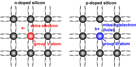
An extrinsic semiconductor is one that is doped with a specific impurity in order to improve the conducting properties. A Experimental top gate capacitance as a function of filling factor for devices with da M 06 08 10 and 15 at the lowest temperature 10 or 20 K allowed by the samplecontact resistance.

Pn Junction Theory For Semiconductor Diodes
Here are two simple animations illustrating how relays use one circuit to switch on a second circuit.
. Best Free Elementor WordPress Themes 2021 Optimized Mobile WooCommerce Theme. TB Wedding Best Free Elementor WooCommerce Theme. For example if you use a 1MΩ resistor for the pull-up R1 and the input pins impedance R2 is on the order of 1MΩ forming a voltage divider the voltage on the input pin is going to be around half of VCC and the microcontroller might not register the pin being in a high state.
TB Camera Best Free Elementor WooCommerce Theme. The frequency response given by the filters transfer function is an alternative characterization of the filter. Both shallow donors and acceptors can form with low formation energies allowing CH 3 NH 3 PbI 3 to be intrinsically doped from p-type to n-type when carefully controlling the growth conditions.
When power flows through the first circuit 1 it activates the electromagnet brown generating a magnetic field blue that attracts a contact red and activates the second circuit 2. This makes the semiconductor suitable for electronic applications like diodes transistors etc. A linear time-invariant LTI filter can be uniquely specified by its impulse response h and the output of any filter is mathematically expressed as the convolution of the input with that impulse response.
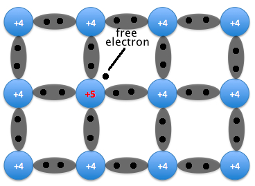
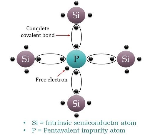
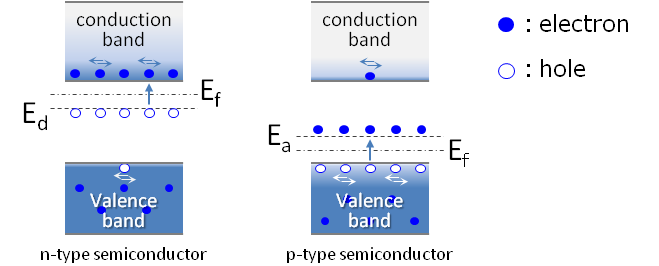
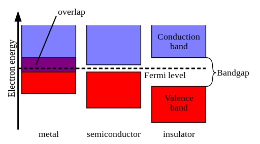
How relays work. The scan cells are linked together into scan chains that operate like big shift registers when the circuit is put into test mode. What is p-type and n-type semiconductorDepending on the kind of impurities added to the semiconductor it becomes either p-type or n-type.
After the test pattern is loaded the design is placed back into functional mode and the test response is captured in one or. Impulse response and transfer function. Rated 500 out of 5.
The scan chains are used by external automatic test equipment ATE to deliver test pattern data from its memory into the device.

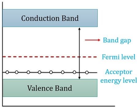
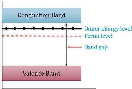
Band Diagram For Activation Energy In N Type Semiconductor Download Scientific Diagram
I P Type N Type Semiconductors Engineering Libretexts

Lesson Explainer Doped Semiconductors Nagwa
Differences Between P Type And N Type Semiconductor Linquip
1 Properties Of Semiconductors Hitachi High Tech Global

Band Bending When A P Type Sc Is Under A E E Fb B E E Fb And C Download Scientific Diagram

Band Diagram For Activation Energy In P Type Semiconductor Download Scientific Diagram
Differences Between P Type And N Type Semiconductor Linquip
Differences Between P Type And N Type Semiconductor Linquip
Why Does An N Type Semiconductor Have Higher Conductivity Quora
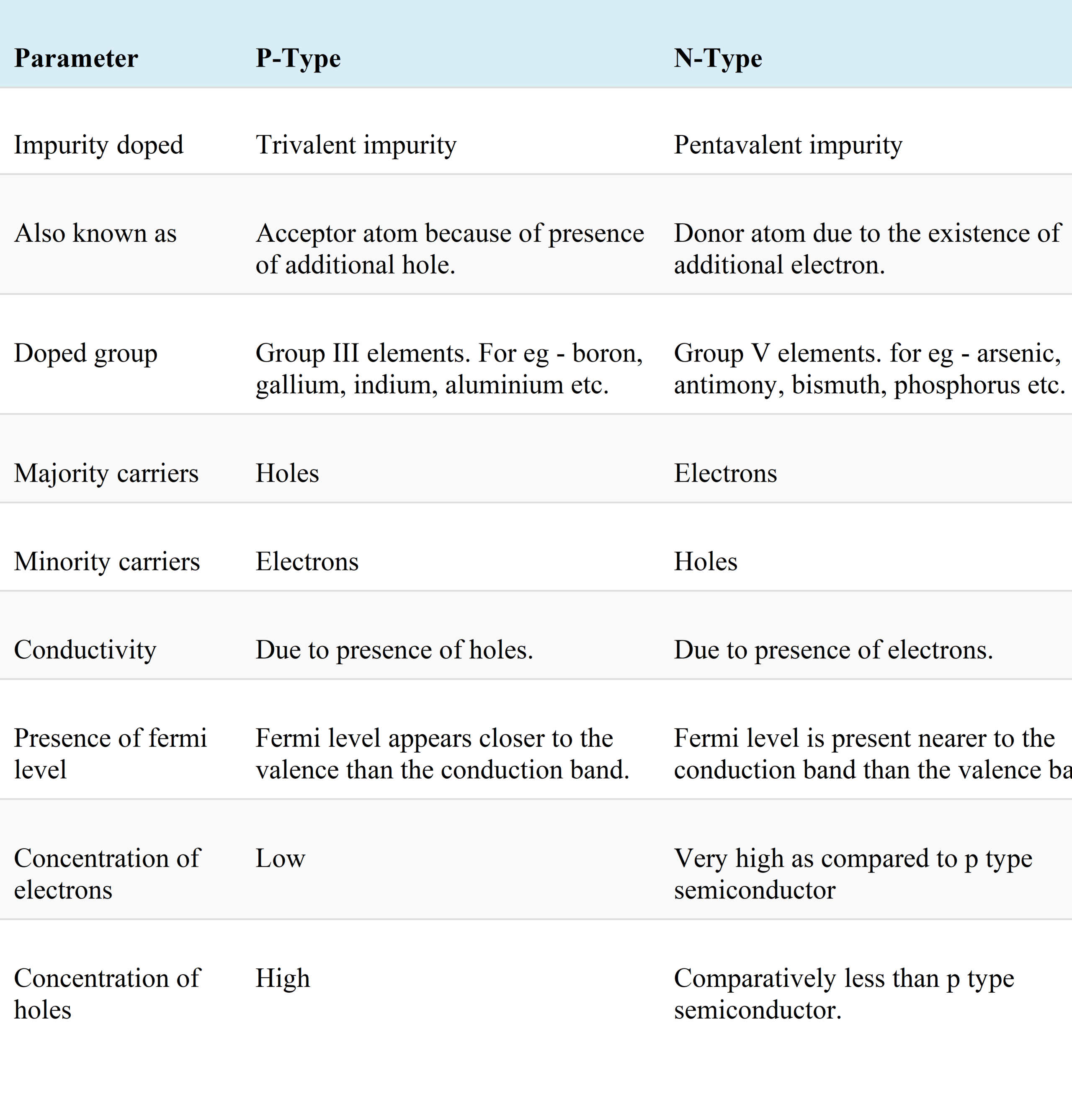
Differences Between P Type And N Type Semiconductor Linquip

A The Structure Model Of The N Type Semiconductor Electrolyte Download Scientific Diagram
Why Does An N Type Semiconductor Have Higher Conductivity Quora
A The Structure Model Of The N Type Semiconductor Electrolyte Download Scientific Diagram
What Are Intrinsic Semiconductors Explain How A Semiconductor Can Be Converted Into An N Type Semiconductor Quora

Mechanism Of Photoelectrocatalysis And The Main Reactions For A N Type Download Scientific Diagram
Differences Between P Type And N Type Semiconductor Linquip
Doping Pveducation
Differences Between P Type And N Type Semiconductor Linquip


Comments
Post a Comment